- 您现在的位置:买卖IC网 > Sheet目录345 > MT48H32M16LFB4-75B IT:C (Micron Technology Inc)IC SDRAM 512MB 54VFBGA
�� �
�
�512Mb:� 32� Meg� x� 16,� 16� Meg� x� 32� Mobile� SDRAM�
�WRITE� Operation�
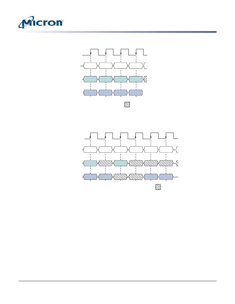
�Figure� 28:� Random� WRITE� Cycles�
�T0�
�T1�
�T2�
�T3�
�CLK�
�Command�
�Address�
�DQ�
�WRITE�
�Bank,�
�Col� n�
�D� IN�
�n�
�WRITE�
�Bank,�
�Col� a�
�D� IN�
�a�
�WRITE�
�Bank,�
�Col� x�
�D� IN�
�x�
�WRITE�
�Bank,�
�Col� m�
�D� IN�
�m�
�Don’t� Care�
�Note:�
�1.� Each� WRITE� command� can� be� issued� to� any� bank.� DQM� is� LOW.�
�Figure� 29:� WRITE-to-READ�
�T0�
�T1�
�T2�
�T3�
�T4�
�T5�
�CLK�
�Command�
�WRITE�
�NOP�
�READ�
�NOP�
�NOP�
�NOP�
�Address�
�Bank,�
�Col� n�
�Bank,�
�Col� b�
�DQ�
�D� IN�
�n�
�D� IN�
�n+1�
�D� OUT�
�b�
�D� OUT�
�b+1�
�Don’t� Care�
�Note:�
�1.� The� WRITE� command� can� be� issued� to� any� bank,� and� the� READ� command� can� be� to� any�
�bank.� DQM� is� LOW.� CL� =� 2� for� illustration.�
�PDF:� 09005aef8459c827�
�512mb_mobile_sdram_y67m_at.pdf� –� Rev.� B� 3/11� EN�
�58�
�Micron� Technology,� Inc.� reserves� the� right� to� change� products� or� specifications� without� notice.�
�?� 2011� Micron� Technology,� Inc.� All� rights� reserved.�
�发布紧急采购,3分钟左右您将得到回复。
相关PDF资料
MT48H8M16LFB4-75 IT:K TR
IC SDRAM 128MBIT 133MHZ 54VFBGA
MTC100-JA2-P34
CONTACT INSERT PIN
MX841BE
IC CONVERTER WHITE LED 8-SOIC
MXHV9910BTR
IC LED DRIVER HIGH BRIGHT 8-SOIC
MXN12FB12F
MOTOR BRUSHED DC 12V 2922RPM
MXN13FB08B1
MOTOR BRUSHED DC 8V 4714RPM
N01L63W2AB25I
IC SRAM ASYNC 1MBIT ULP 48-BGA
N01L63W3AB25I
IC SRAM 1MBIT 3V LP 48-BGA
相关代理商/技术参数